Hardware for sensing digital test indicators
In a typical machine shop dial test indicators are widely used, for checking alignment, concentricity and general measurements. Often classical mechanical ones are used, but today there also exist digital ones.
One example is the TESA Twin T10, I would say that the biggest benefit is that you can place the display at a distance (how long the cable is), maybe outside of the machine cover and more easily read the results.
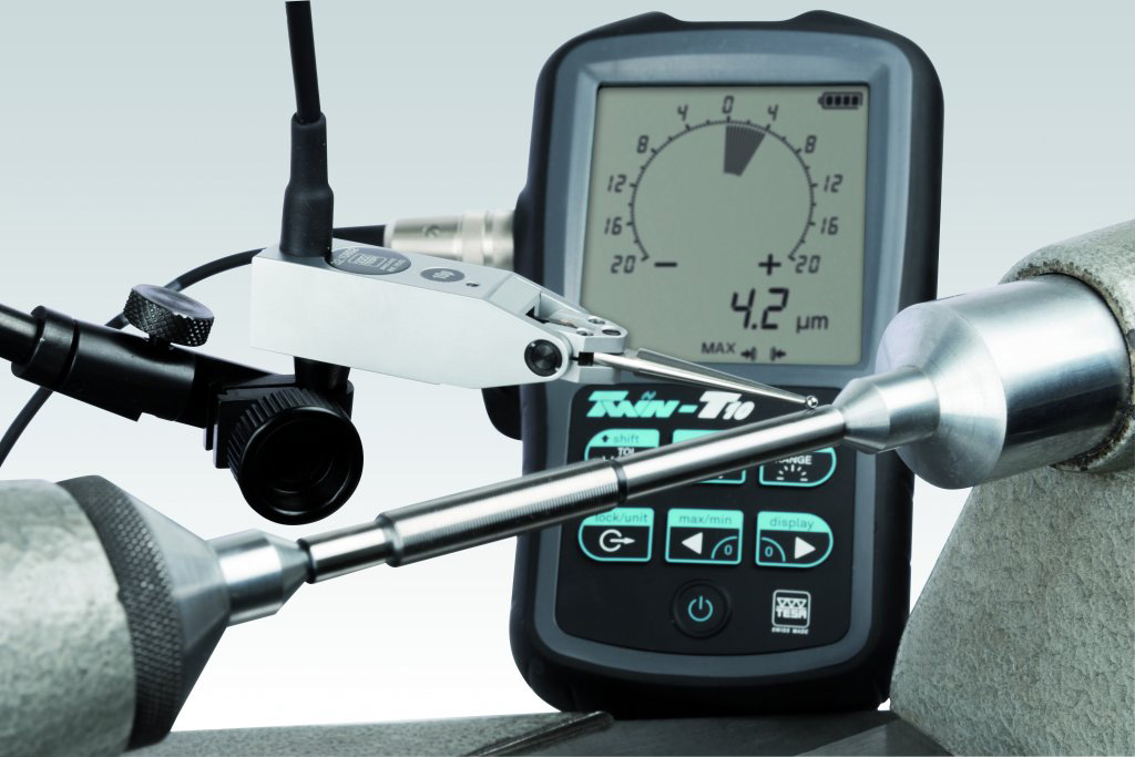
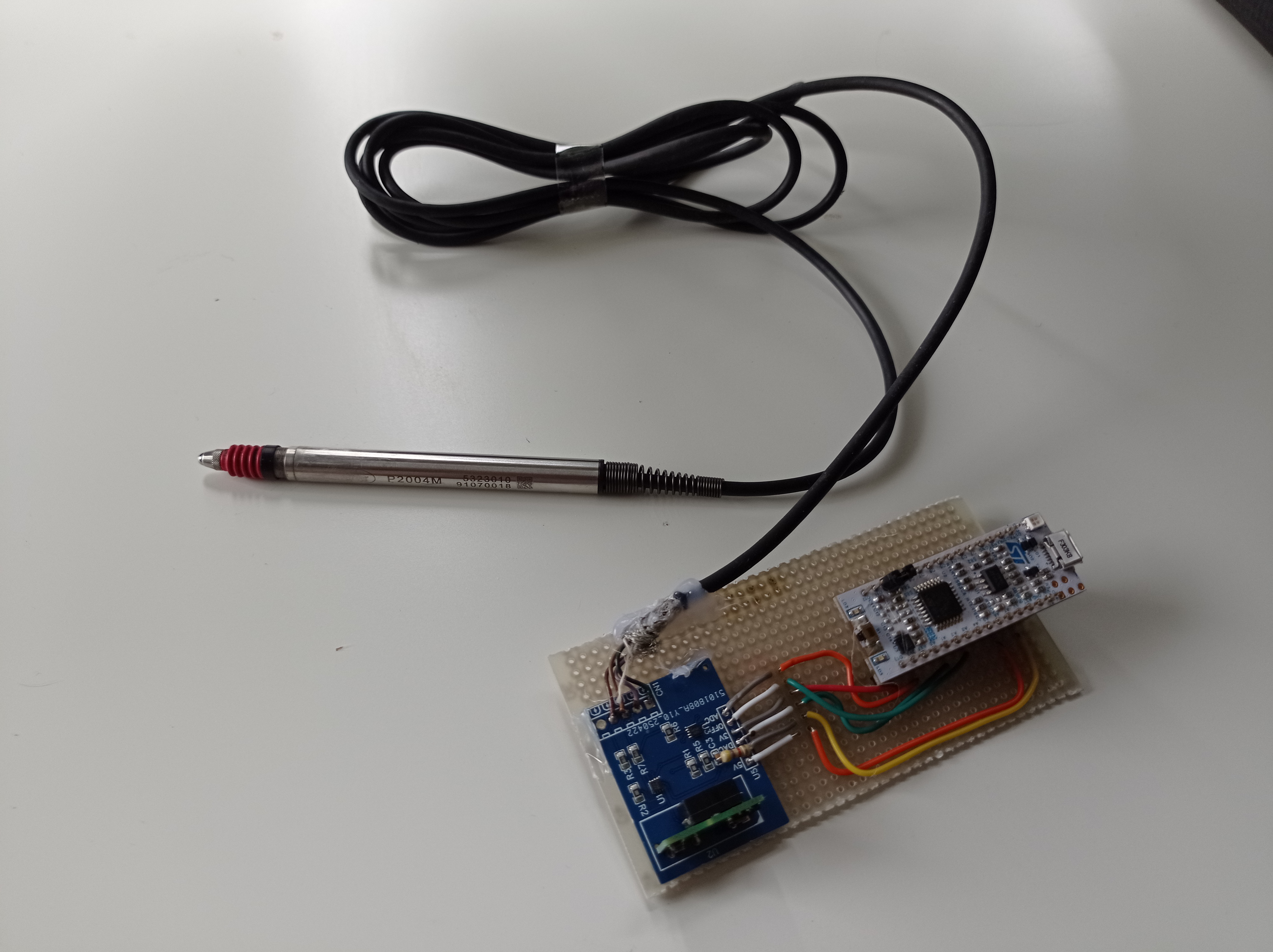
I’ve always wondered how these measurement probes work, and I’ve always assumed that it was some sort of analog signal. Recently I’ve gotten my hands on an old probe that was to be scrapped and thought that it would be perfect to try and build my own sensor reader/display.
After some initial research I learned that the sensor used is a linear variable differential transformer (LVDT). I really liked the animations from this website https://www.rdpe.com/ex/hiw-lvdt.htm
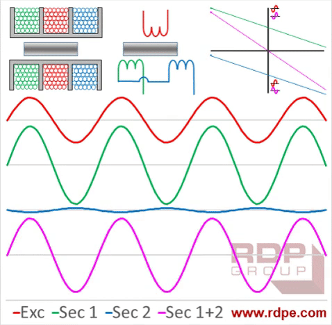
They explain the general principle of a LVDT, which essentially has an input voltage and a output voltage. The measuring circuit sends out an excitation sine wave and the LVDT returns a sine wave where the amplitude is dependent on the position of the probe.
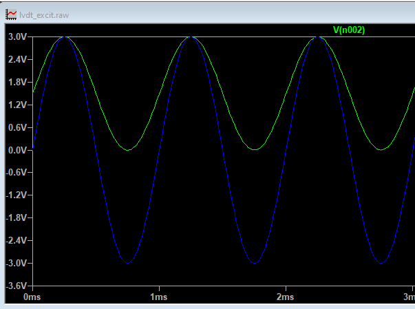
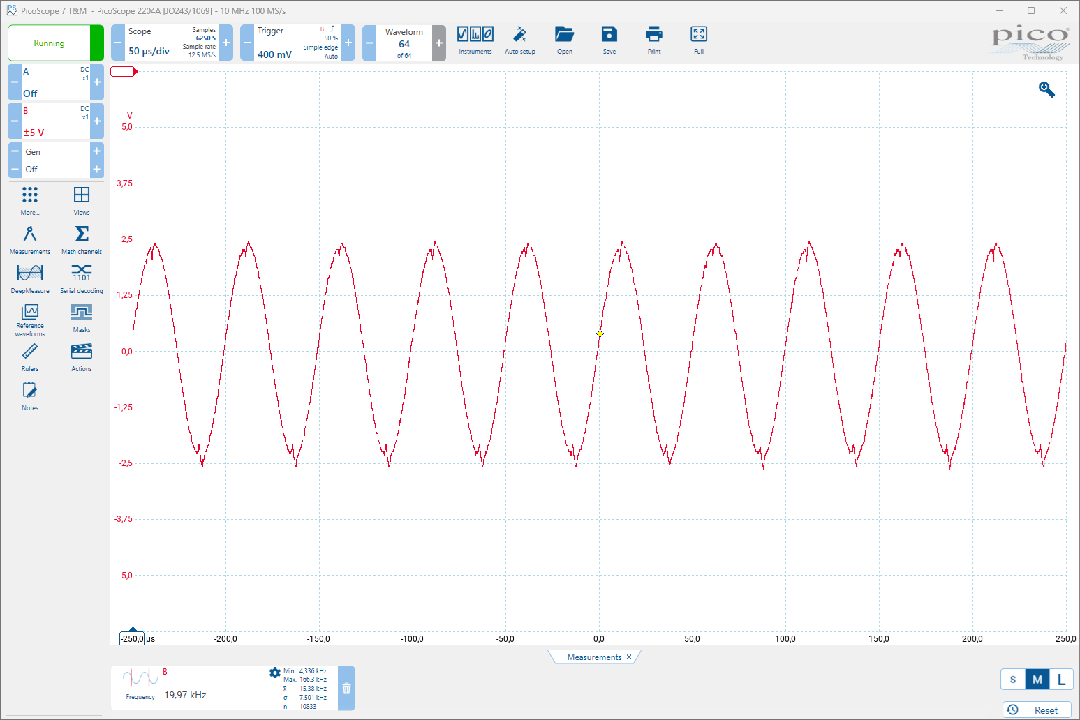
So far there is plenty of information for the principle of LVDT’s, but as soon as you try and find values of the voltages it gets more difficult. So I connected an oscilloscope and measured the excitation signal and the resulting sensing signal.
I assume that most probes are compatible with different measurement units, in my case I have a Mahr probe but the display unit is a Sylvac D70I. For this display, the excitation signal was 19.7 kHz and with an amplitude of 3V, the sense signal had a maximal amplitude of 0.5V.
An overview of the voltages is shown below.

Hardware
After figuring out the signal characteristics it was just a question of how to scale the signals to suit the DAC and ADC of a microcontroller. And also how the microcontroller can handle the high frequency of the signals.
I started with designing a board for handling the scaling and offsetting of the signals to work with a 3.3V STM Nucleo board. The plan is that the MCU generates a sine wave from its DAC and samples the sensing signal on its ADC.
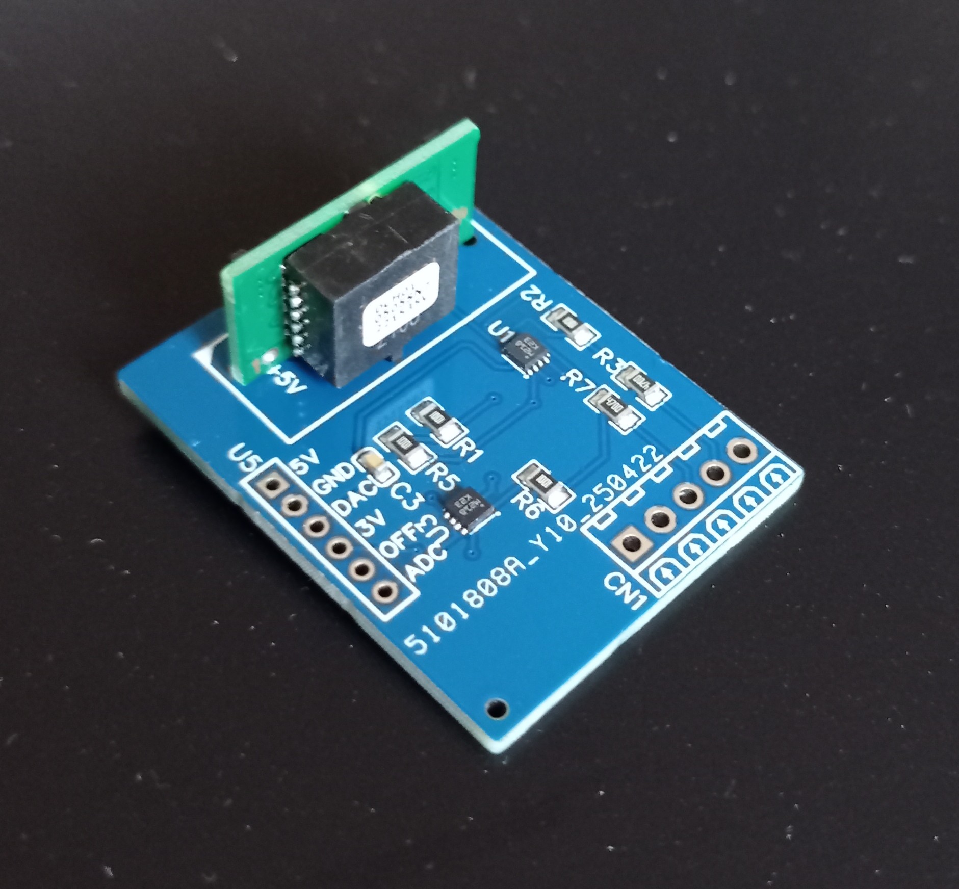
For this project I also thought it would be cool to try out a PCB assembly service. Since I decided to use JLC-PCB I used their online PCB design tool, which worked surprisingly well. There I could design the circuit and pick out components from their assembly service.
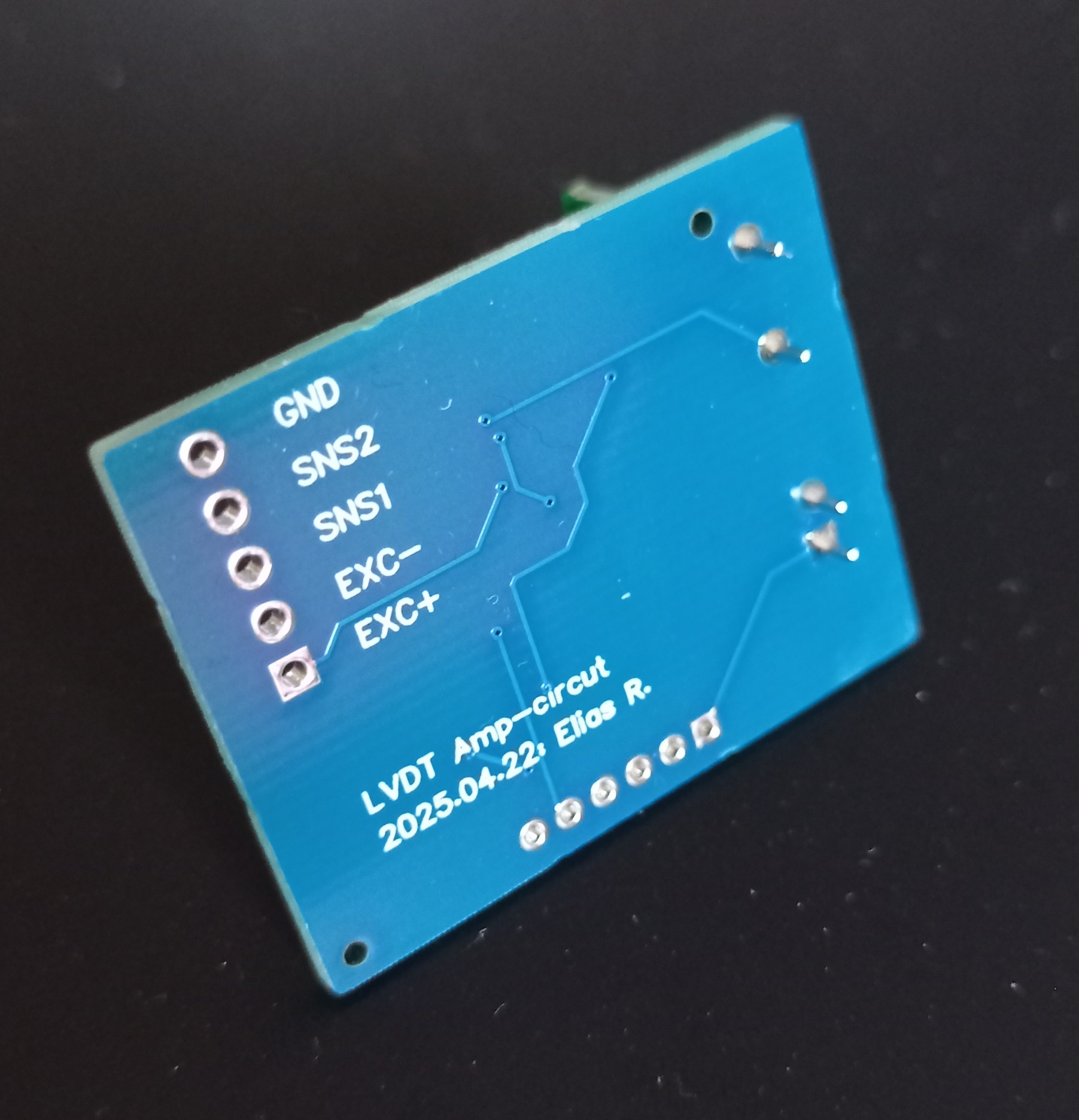
The final circuit can be seen here, note that this is rev 1.1, I forgot one of the resistors that I had to patch on the final PCB.
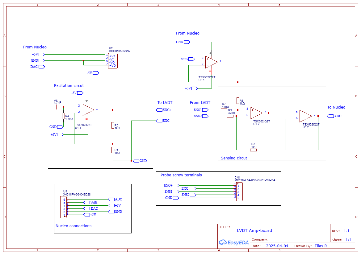
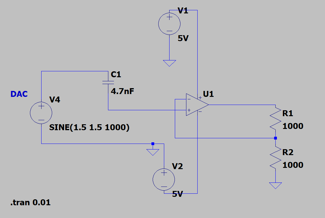
In order to scale and offset the analog voltages I use OP-amps, there is plenty of information online of how to use them to scale signals. But in order to just scale a signal, amplify it, one could use a non-inverting amplifier circuit. It consits of an OP-amp and two resistors.

In this circuit, the gain can be calculated as
\[\frac{V_{out}}{V_{in}} = 1 + \frac{R_1}{R_2}\]One thing that I did not know before starting this project was that a standard OP-amp cannot drive its output voltage to its supply voltages (rail voltage).
Before ordering the final PCB I ran some tests in LTSpice, a simulation software to verify that I calculated the correct values for the resistors. One can really dive deep into this, specifying all the electrical characteristics of the OP-amps, etc. For me it was good enough with ideal theoretical components.
If you want OP-amps that behave similar to ideal OP amps, that can drive the output close to the supply voltages, you need rail to rail OP-amps. The biggest advantage of using rail to rail amps in this application, is that by feeding the OP-amp that scales the ADC-input voltage with 3.3V it’s impossible to send a voltage greater than 3.3V to the ADC, thus not risking sending an over-voltage to the MCU.
Software
Going in to this project I knew that the most difficult part of the software would be to get the sine wave generation and ADC sampling running fast enough.
Simply writing to the ADC from a for-loop with 64 points can only achieve a frequency of 5.1 kHz, and this is without sampling and any processing. So this frequency would only get lower when adding more functionality.
Luckily there exists something called Direct Memory Access (DMA) on the Nucleo, this means that you can configure a timer event to trigger a copy from a memory buffer to the DAC and start the conversion, all done by the hardware without the need of the CPU. Thus achieving way higher frequencies. The same method is used for the ADC sampling, and using the same timer event, results in that the ADC sampling is always synchronized with the DAC signal generation.
Then when evaluating the resulting sense signal, I knew that I wanted to do some kind of least squares estimate of a sine wave in order to compute the measured value. This would be max 10 lines in python to do, but I wanted to do it on the MCU for two reasons:
I would be able to run the measurement at a higher rate and possibly filter the measured value If I wanted to read the measurement to another low-level programming device, like a PLC, it would be much easier to just request a value.
For the least squares estimate I define the sense signal from 3 parameters, amplitude, phase and offset.
\[V_{sns}(t) = A_s \sin(\omega t + \phi)\]This can also be expressed as a sum of sin/cos and an offset which makes this linear in the parameters.
\[V_{sns}(t) = a_0 \sin(\omega t) + a_1 \cos(\omega t)\]where the original parameters can be found by
\[\hat A_s = \sqrt{a_0^2 + a_1 ^2}\] \[\hat \phi = \texttt{atan2}(a_1,a_0)\]This does pose one problem, \(A_s\) is always positive, and \(\phi\) adjusts in order to accommodate the sign change of \(A_s\), I solved this by simply checking what phase \(V_{sns}\) had in the positive direction and negative direction, because in theory the phase should be 180 degrees apart in the negative and positive range.
Assume that when measuring a positive value, \(\phi = 60^\circ\) then I calculate the Amplitude with sign as
measValue = amp;
if((phase > 150*3.14/180.0) || (phase < -30*3.14/180.0)){
    measValue = measValue*-1;
}
The final least squares problem will be to identify the amplitude, phase and offset. Given \(N\) measurements and the angular velocity \(\Omega\), we need to solve
\[M \theta = Y\] \[M = \begin{bmatrix} 0 & 1 & 1 \\ \sin(\Omega) & \cos(\Omega) & 1 \\ \sin(2\Omega) & \cos(2\Omega) & 1 \\ \sin(3\Omega) & \cos(3\Omega) & 1 \\ \vdots & \vdots & \vdots \\ \sin((N-1)\Omega) & \cos((N-1)\Omega) & 1 \\ \end{bmatrix}\] \[\begin{bmatrix} y_0 \\ y_1 \\ y_2 \\ y_3 \\ \vdots \\ n_{N-1} \end{bmatrix}\]One easy solution is to use the pseudo inverse by multiplying each side with \(M^T\)
\[M^T M \theta = M^T Y\] \[\theta = (M^T M)^{-1} M^T Y\]My first plan was to use the Eigen library, that makes it possible to work with matrices and vectors in C++. However I quickly realized that the eigen library was to large to fit on the MCU so I was forced to either find a more lightweight library or simply write the matrix operations myself. Since it only was a 3x3 matrix that needed inverting, I thought that it would be feasible to code the analytical inverse. For this I used a jupyter notebook for prototyping in python, which can be found on my Github: https://github.com/eliasrhoden/Measurement-indicator/blob/main/lvdt_probe_least_squares.ipynb
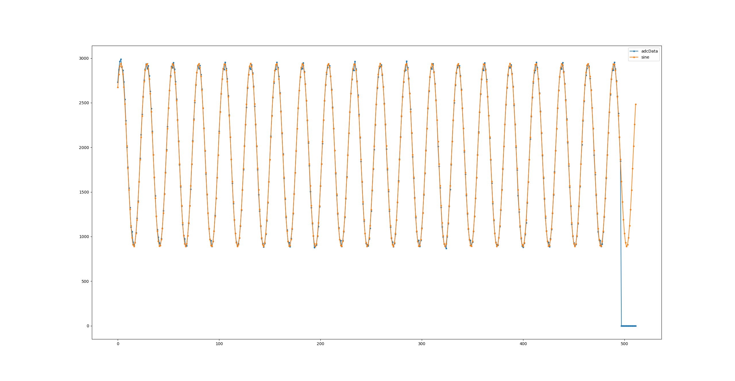
After getting a working prototype working in python it was straightforward to port it to c and run it on the MCU. The last thing that I needed to do was to implement a simple interface of the serial COM port and the corresponding PC-client.
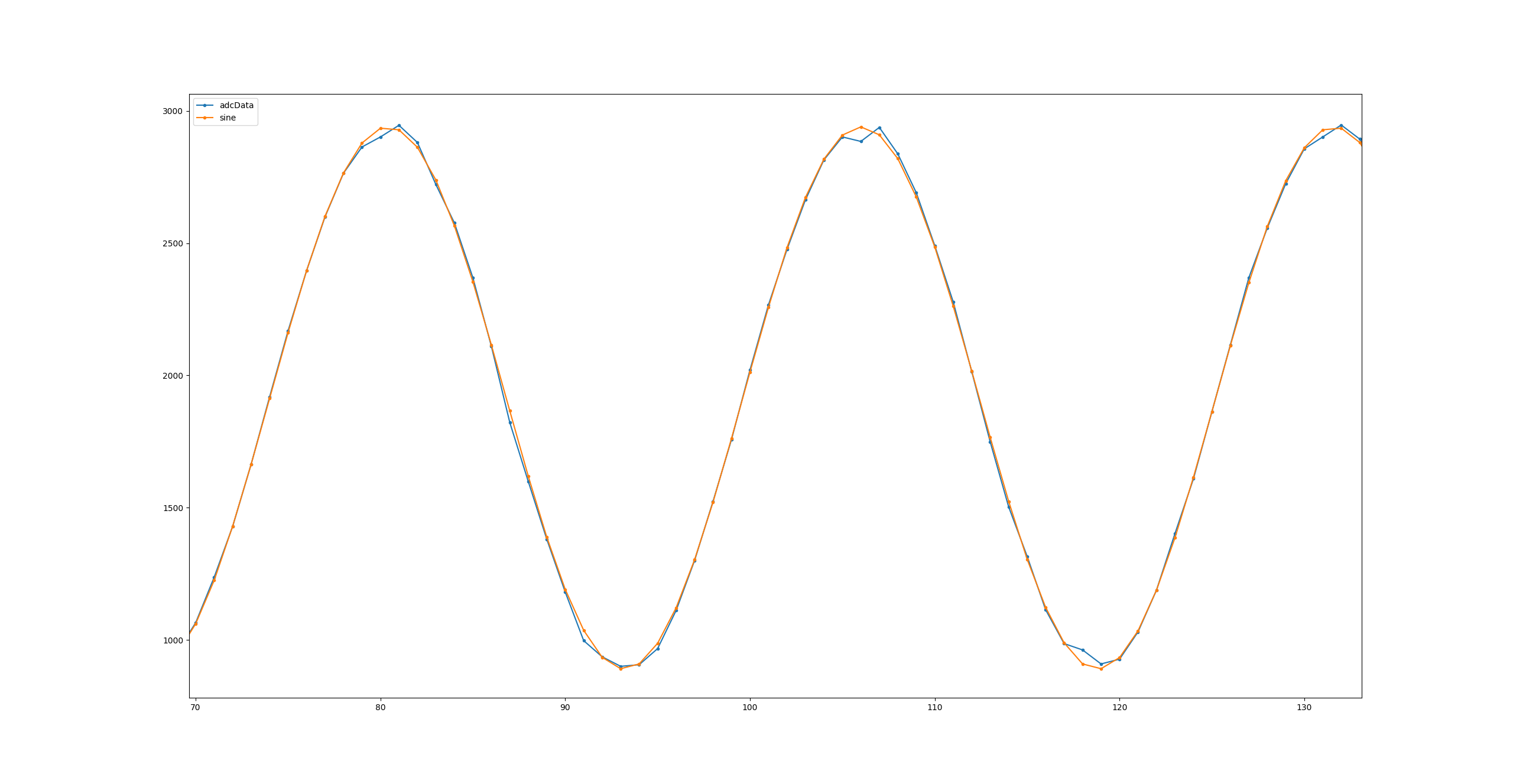
With the client one can see the sampled sense signal from the ADC and the estimated since wave, there are still some flickering in the phase of the signal due to ADC/DAC timing, but this is only equivalent to less than 5 degrees, and since the Amplitude determines the measured value this does not seem to affect the measurement too much.
Final prototype
I’m quite happy how the final prototype turned out, you can see the extra resistor I had to patch in on my amplification board, but other than than it was straight forward to solder.
I noticed that the generated sine wave from the DAC looks really good, but the amplified signal going to the excitation coil has some noise at its peaks, and I think this shows in the sampled ADC signal as well. This noise was reduced when I lowered the amplitude of the generated sine-wave, so the noise was reduced at the cost of resolution, since I no longer utilize the full voltage range (+/- 3V).
If I were to do a second version of this board I would include some hardware LP filter on the excitation signal and also on the sense signal, in order to reduce the overall noise.
The most expensive part on the board was the 5V regulator, trying to find a cheaper one would probably reduce the assembled PCB cost quite a bit. Also I picked the wrong type of header spacing, thus the extra cables between the PCB and perfboard. I would add some headers to plug in the Nucleo directly to the PCB as well, to avoid the need of a perfboard. And lastly the PCB traces could probably be routed better in terms of improved EMC robustness.
Conclusion
To wrap up this blog post I would call this a success, this was one of those project where the overall plan was simple, but a lot of new techniques and process that I had never done before myself, especially designing the amplification board.
As usual, the code and schematics can be found on my Github: https://github.com/eliasrhoden/Measurement-indicator